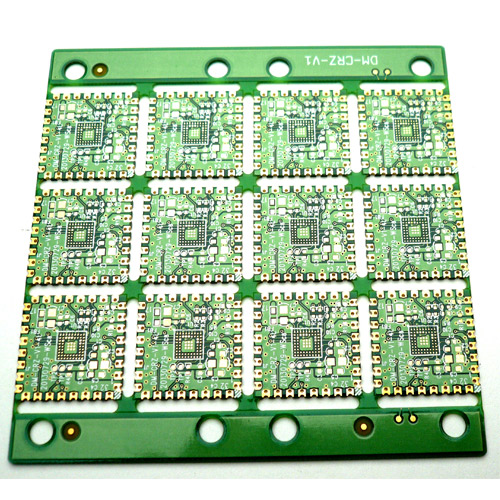
The idea of IoT (Internet of Things) is getting more and more popular, nowadays everything can be connected to the internet. However, portable devices which people wear or carry everyday must be as small as possible.
In order to shrink the size of PCB, PCE offer Via in Pad process to our clients. We fill up the PTHs (Plated Through Holes) with conductive (or non-conductive) epoxy, and copper-plating the surface of each via hole.
 |
 |
 |
 |
 |
Applications & Benefits:
- Tighter BGA pitches
- Increased thermal dissipation
- Reduced layer count or board size, which ultimately may reduce cost
- Improved routing density (higher density per layer)
- Strengthening Pad attachment
- Gives high frequency designs the shortest possible route to bypass capacitors
- Overcomes high speed design issues and constraints such as low inductance
Rigid PCB Capability
| Feature | Capability | |
|---|---|---|
| Lamination | Layer count | 1-32 layers |
| Min. thickness | 4 mil(0.1 mm) | |
| Max working panel size | 24x31.5 inch(610x800mm) | |
| Max. aspect ratio | 10:1 | |
| Copper | Copper Thickness | 0.33~3.0 oz (11~105um) |
| Trace | Min. Line Width /Space | 3/3 mil |
| Routing | Dimension tolerance | +/- 2 mil (0.05mm) |
| Solder Mask | S/M minimum dam width | 2.5 mil |
| Impedance Control | Differential pair | +/- 10% |
| Mechanical Drilling | Min. drilling hole size | 4 mil(0.1mm) |
| 3 Axis | Depth control accuracy | +/- 2mil (0.05mm) |
| Material Availability | FR-4, High Tg FR-4, Halogen-free FR-4, Metal Core, Low Dk/Df (ISOLA/ Rogers) | |
| Finish Availability | Lead-free HASL, HASL, OSP, ENIG, Pattern Gold Plating, Immersion Silver/Tin, Carbon Ink | |

